
Person in Charge
Hasdiyana Hashim
Tel : +603-5543 7903
Email : hasdiyana2370@uitm.edu.my
Centre :
CENTRE FOR FUNCTIONAL MATERIALS & NANOTECHNOLOGY (CFMN)
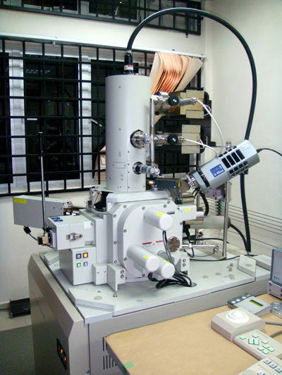
Field emission scanning electron microscopy (FESEM) provides topographical and elemental information at magnifications of 10x to 300,000x, with virtually unlimited depth of field. Compared with convention scanning electron microscopy (SEM), field emission SEM (FESEM) produces clearer, less electrostatically distorted images with spatial resolution down to 1 1/2 nanometers – three to six times better.
Other advantages of FESEM include:
- The ability to examine smaller-area contamination spots at electron accelerating voltages compatible with energy dispersive spectroscopy (EDS).
- Reduced penetration of low-kinetic-energy electrons probes closer to the immediate material surface.
- High-quality, low-voltage images with negligible electrical charging of samples (accelerating voltages ranging from 0.5 to 30 kilovolts).
- Essentially no need for placing conducting coatings on insulating materials.
- For ultra-high-magnification imaging, we use in-lens FESEM.
Model : JSM - 7600F
Brand : Jeol
General sample requirements/prerequisites and rules:
1. Preliminary discussions regarding samples and techniques must first be done with the head of Centre.
2. A guarantee letter must be given, addressed to the Head of Centre.
3. The sample must be pure. The phases must have been identified and proof of this must be given.
4. The sample must be stable (not reactive, toxic or corrosive)
5. The sample must be very dry in order to be placed in high vacuum.
6. All payments must be made before results can be taken.